Update from the excellent researcher ‘Tuomo’, with some more revised observations;
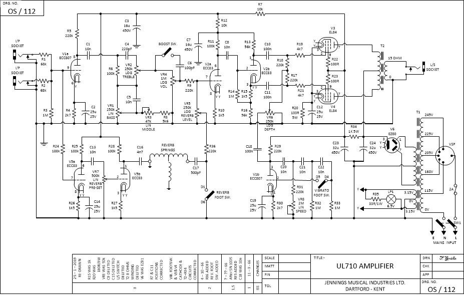
UL710 schematic
The known schematics
There are two known UL710 schematics at the moment. The official JMI schematic OS/112 issue 2 dated at 4 – 10 – 66 and the other called ‘Un-numbered’.
Jim Elyea published the OS/112 in his ’Vox bible’. It indicates a couple of changes to the original first issue that was released at 11 – 3 – 66. Unfortunately, there are still number of errors in the schematic and maybe for that reason someone started to re-draw the schematic taking the actual amp circuit as reference.
The un-numbered version also has errors, and it seems that it is just a draft which wasn’t ever finalised. This schematic is following the actual built amps more precise though.
These two schematics have different component numbering. In OS/112 the numbering is based on the drawing itself, starting from upper left corner towards the lower right corner. The numbering in the other schematic follows more the positioning of the components in the tag board and placing of the tubes in chassis. I am referring to the numbering of OS/112 in this article.
Since the both schematics have mistakes, I decided to reverse engineer the mystery and re-draw the OS/112 schematic based on my own amp SN 1005. While doing that I noticed some additional changes that hasn’t been documented in issue 2.
The changes before issue 2
The Issue 2 states two changes: addition of R36 and Reverb footswitch.
My amp SN 1005 is one of the first ever made, if serial numbering started from 1000 or 1001. It represents the circuit that should have been documented in the first version. It has two other differences than those mentioned in Issue 2: Also R35 is missing and value of capacitor C18 is 10nF.
In later amps C18 was changed to 100nF and they all have those two additional resistors R35 and R36 as shown in Issue 2 schematic. All amps have had a two-button footswitch which controls reverb and vibrato. It means that the missing footswitch was just a drawing error.
I marked the R35 and C18 related changes as ’issue 1,5’.
The other errors in OS/112
As mentioned earlier there are errors in the OS/112 Issue 2 schematic.
Quite many errors are related to A+ voltage circuit. All amps seem to have EZ80 rectifier tube, so I changed that. Next in line is the point where the A+ voltage is taken to the center of the output transformer’s primary winding. It is taken directly from the EZ80, not after R34. Also position of R10 was incorrect, now it is in position as in the actual circuit. It feeds A+ voltage to all preamp ECC triodes, except V1b which gets A+ voltage through R29.
I deleted two cathode capacitors C9 and C15 since they are not installed to any of the amps.
Position of coupling capacitor C11 was also drawn incorrectly. It is connected directly to V2b cathode, not to the other end of R15. Value of R15 is also changed to the one in amps (1k5).
Another mistake was in V3 and V4 cathodes which were not connected to each other as they should. I also changed the value of the cathode resistor R20 to the one in amps (133R / 5W).
Also, the vibrato oscillator circuit is now fixed. The change is related to the position of the footswitch. If you do not own the footswitch, then your vibrato isn’t working, since you need it for shortcutting the oscillator circuit.
The last changes are the loudspeaker switch and 8 ohms winding in T2 that I deleted, because UL710 has only 15 ohms output and switch is missing.
I have listed all corrections that I made to re-drawn ‘issue 3’. I have also drawn another picture that shows the components in the main tag board. I hope that these two pictures give you some help with your amps. I have tried to check everything for avoiding to creat any new errors, but I cannot be 100% sure if everything is correct.
NOTE: I DON’T TAKE ANY RESPONSIBILITY OF THE USAGE OF THE PICTURES, THEY ARE DRAWN ONLY FOR INFORMATION PURPOSES AND THEY CAN STILL HAVE ERRORS. WORKING WITH AMP WHEN CHASSIS IS TAKEN OUT FROM THE CABINET IS DANGEROUS DUE TO HIGH VOLTAGES. LET YOUR ENGINEER DO THE WORK!